| |
Maxim Integrated - 400mV 到 5.5V 輸入, nanoPower 具真實關閉同步式昇壓轉換器
The MAX17220–MAX17225 is a family of ultra-low
quiescent current boost (step-up) DC-DC converters with
a 225mA/0.5A/1A peak inductor current limit and True
Shutdown™. True Shutdown disconnects the output from
the input with no forward or reverse current. The output
voltage is selectable using a single standard 1% resistor.
The 225mA (MAX17220), 500mA (MAX17221/MAX17222/
MAX17223), and 1A (MAX17224/MAX17225) peak inductor
current limits allow flexibility when choosing inductors. The
MAX17220/MAX17222/MAX17224 versions have poststartup
enable transient protection (ETP), allowing the
output to remain regulated for input voltages down to
400mV, depending on load current. The MAX17220–
MAX17225 offer ultra-low quiescent current, small total
solution size, and high efficiency throughout the entire load
range. The MAX17220–MAX17225 are ideal for battery
applications where long battery life is a must.
Features
• 300nA Quiescent Supply Current Into OUT
• True Shutdown Mode
• 0.5nA Shutdown Current
• Output Disconnects from Input
• No Reverse Current with VOUT 0V to 5V
• 95% Peak Efficiency
• 400mV to 5.5V Input Range
• 0.88V Minimum Startup Voltage
• 1.8V to 5V Output Voltage Range
• 100mV/Step
• Single 1% Resistor Selectable Output
• 225mA, 500mA, and 1A Peak Inductor Current Limit
• MAX17220: 225mA ILIM
• MAX17221/MAX17222/MAX17223: 500mA ILIM
• MAX17224/MAX17225: 1A ILIM
• MAX17220/MAX17222/MAX17224 Enable Transient
• Protection (ETP)
• 2mm x 2mm 6-Pin μDFN
• 0.88mm x 1.4mm 6-Bump WLP (2 x 3, 0.4mm Pitch)
Application
• Optical Heart-Rate Monitoring (OHRM) LED Drivers
• Supercapacitor Backup for RTC/Alarm Buzzers
• Primary-Cell Portable Systems
• Tiny, Low-Power IoT Sensors
• Secondary-Cell Portable Systems
• Wearable Devices
• Battery-Powered Medical Equipment
• Low-Power Wireless Communication Products
Product Benefits
• 低靜態電流With just 300nA of quiescent current
• 適穿戴式產品ideal for battery-powered wearables
• 單一外部電阻可決定32段不同VOUT,傳統要2顆, program the output voltage with a single resistor
• 銅板大小電路配上高阻抗電池仍能啟動並運作自如 ,ability to start up and operate with high source impedance batteries
(such as coin cell or smaller).
• 高輸出電流500mA, higher output currents
• 外部零件只要4顆
• 400mV to 5.5V 輸入
Specifications
• OUT, EN, IN to GND................................................-0.3V to +6V
• RSEL to GND................. -0.3V to Lower of (VOUT + 0.3V) or 6V
• LX RMS Current WLP...............................-1.6Arms to +1.6Arms
• LX RMS Current μDFN...................................-1Arms to +1Arms
• Continuous Power Dissipation (TA = 70°C)
• WLP (derate 10.5mW/°C above +70°C).......................840mW
• Continuous Power Dissipation (TA = 70°C)
• μDFN (derate 4.5mW/°C above +70°C)....................357.8mW
• Operating Temperature Range............................ -40°C to +85°C
• Junction Temperature.......................................................+150°C
• Storage Temperature Range............................. -40°C to +150°C
• Soldering Temperature (reflow)........................................+260°C
Block Diagram
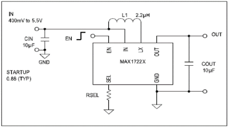
• OUT Output Pin. ----Connect a 10μF X5R ceramic capacitor (minimum 2μF capacitance) to ground.
• LX Switching Node Pin. ----Connect the inductor from IN to LX.
• GND ----Ground Pin.
• EN Active-High Enable Input. -----See Supply Current section for recommended connections.
• IN Input Pin. -----Connect a 10μF X5R ceramic capacitor (minimum 2μF capacitance) to ground.
• Depending on the application requirements, more capacitance may be needed (i.e., BLE).
• SEL Output Voltage Select Pin. ----Connect a resistor from SEL to GND based on the desired
Web Buyable:
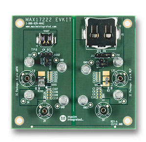
https://www.maximintegrated.com/en/products/power/switching-regulators/MAX17222EVKIT.html
Learn More:
https://www.maximintegrated.com/en/products/power/switching-regulators/MAX17220.html
https://datasheets.maximintegrated.com/en/ds/MAX17220-MAX17225.pdf

▲回頁首
|
|
|